View Images Library Photos and Pictures. US20060225007A1 - Antenna effect prevention by model extraction in a circuit design for advanced processes - Google Patents Errors due to process variations - ppt download Antenna effect in VLSI Fabrication | Plasma Induced Gate Oxide Damage | Plasma Etching Antenna effect in VLSI
. Antenna Effect | Capacitor | Diode Antenna Effect in 16nm Technology Node Diodes in antenna effect | Forum for Electronics
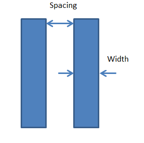
 Process Antenna Rule – sarvangsanghavi
Process Antenna Rule – sarvangsanghavi

 Antenna effect - Wikipedia
 Antenna Effect in 16nm Technology Node

 ⨘ } VLSI } 8 } Antenna Effects } - YouTube
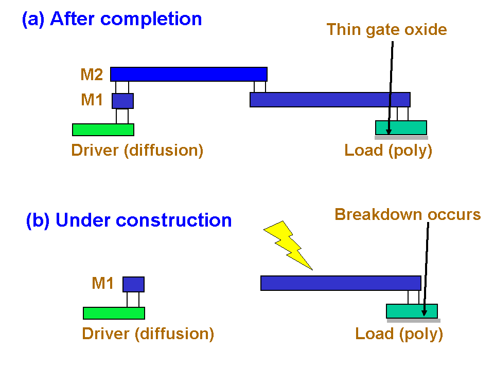
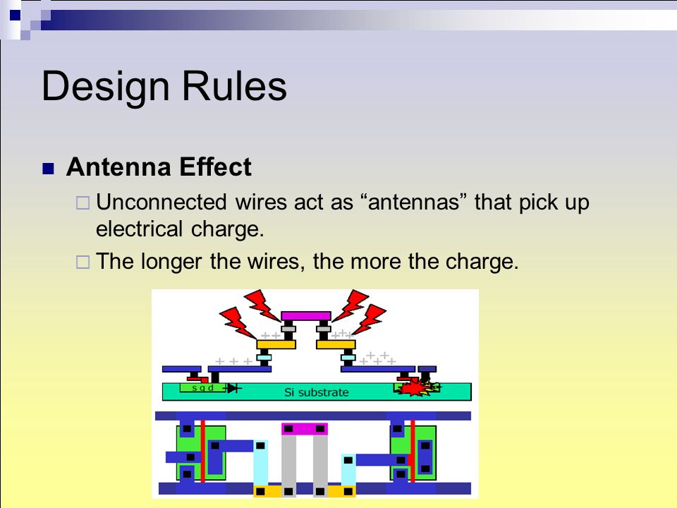
 Errors due to process variations - ppt download

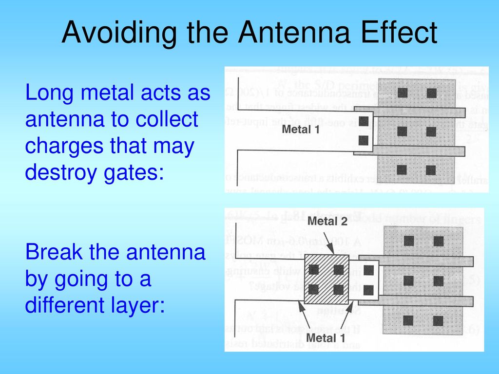
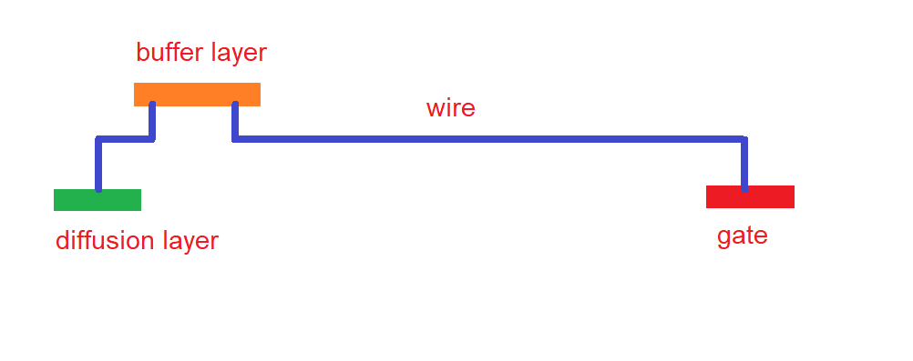
 Mitigating antenna effect in IC design(2)
 PDF) The Antenna Effect: Problem and Solutions | A Đỗ Tấn - Academia.edu
OSA | Array of plasmonic Vivaldi antennas coupled to silicon waveguides for wireless networks through on-chip optical technology - WiNOT
 Explain Antenna Effect
 vlsi mcq questions 28.12
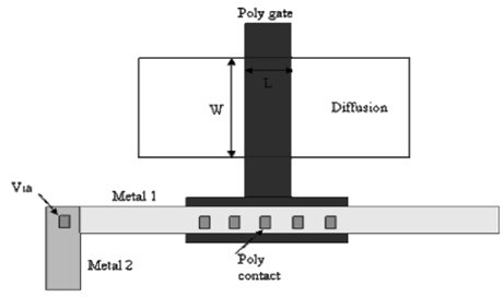
 Full-Custom Design …. TYWu. Outline Introduction Transistor Process Steps Layout Schematic R/C Design Rules Tools. - ppt download
 Mitigating antenna effect in IC design(3)
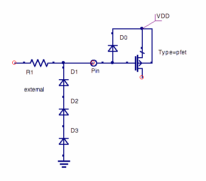
 Antenna violations resolved using new method - EDN
 Antenna effect in VLSI
 Antenna effect in VLSI Fabrication | Plasma Induced Gate Oxide Damage | Plasma Etching - YouTube
 Mitigating antenna effect in IC design(2)
 Antenna effect in VLSI
 Mitigating antenna effect in IC design(2)
 Understanding Antenna in Package Design - AnySilicon
 Addressing Reliability in Physical Design | SpringerLink
 PDF) Layer reassignment for antenna effect minimization in 3-layerchannel routing
Comments
Post a Comment